Manufacturing of optics

We offer fabrication service of micrometer and nanometer scale features.
The service includes design, fabrication, and evaluation of a product. We offer the full fabrication chain, or a part, such as fabrication according to the customer design.
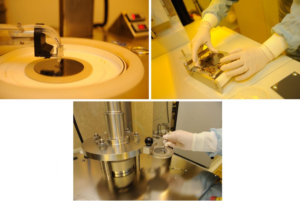
We use electron beam writing and various supplementary lithographic techniques in our fabrication process at cleanroom environment.
Application areas include optical, tactile, tailored, and functional surfaces utilizing micrometer and nanometer scale features.
Our equipment includes:
- Raith EBPG5000+ES electron beam writer
- LAB18 Physical Vapour Deposition system
- Quorum Q300T sputter coater
- Beneq TFS-200 Atomic Layer Deposition system
- Oxford Instruments PlasmaPro 100 Cobra and Plasmalab 80 RIE/ICP etching systems
- Obducat EITRE-3 Nanoimprint lithography system
- Jenoptik EFNI-01 Nickel electroplater
Our methods include:
- Electron beam lithography
- Thin film deposition
- Evaporation
- Sputtering
- Atomic Layer Deposition (ALD)
- Etching
- Reactive ion etching (RIE)
- Wet etching
- Replication
- Nanoimprint lithography (NIL)
- Hot embossing
- Roll-to-roll imprinting
- Nickel electroplating
Contact person:
Pertti Pääkkönen, Senior Laboratory Manager
e-mail: [email protected]
tel: +358 50 505 6376
Pertti Pääkkönen – UEF Connect
We offer fabrication service of directly printed optical elements
The service includes design, fabrication, and evaluation of a product. We offer the full fabrication chain, or a part, such as fabrication according to the customer design.
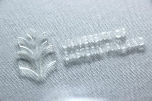
We use direct 3D printing based on inkjet technology.
Application areas include free-form optical components made of acrylic-like polymer. The method is ideal for prototyping purposes.
Our equipment includes:
Custom inkjet 3D printer
Contact person:
Petri Karvinen, Research Manager
e-mail: [email protected]
tel: +358 50 324 7678
Petri Karvinen – UEF Connect
