Photonics materials
Carbon nanomaterials
Keywords: 2D materials; carbon based nanomaterials; light emitting molecules; metamaterials; THz optics; nonlinear optics; nanomaterials; carbon; graphene; nanodiamonds; diamond microneedles; graphene; pyrolytic carbon; carbon nanotubes forest; thin carbon film
The group belongs to the Department of Physics and Mathematics and the Center for Photonics Sciences. It is also a member of the Academy of Finland’s Flagship on Photonics Research and Innovation (PREIN).
Research on carbon materials at the Center for Photonics Sciences is based on the unique methodology and facilities created at Department of Physics and Mathematics. Our research facilities allow us to produce thin film carbon materials with different structural characteristics and physical properties, including single and multilayered graphene with controlled grain size, graphene nano-walls, pyrolytic carbon, graphitized pyrolyzed photoresist (hot wall chemical vapor deposition, CVD), nanodiamond films and single crystal diamond needles, and graphene nano-scrolls (plasma enhanced CVD, PE CVD). Different pre- and post-treatment methods are developed to obtain materials with prescribed morphological and physical properties. The developed at our laboratory technology, which is based on the combination of the PE CVD with thermal oxidation, enables scalable fabrication of unique single crystal diamonds having needle-like shape that are currently attracting a lot of attention in quantum research.
Contact persons:
- Prof. Polina Kuzhir
- Dr. Sergei Malykhin
- Prof. Yuri Svirko
- Prof. Alexander Obraztsov
- Dr. Georgy Fedorov
Selected publications:
- G. Dovbeshko, V. Romanyuk, D. Pidgirnyi, V. Cherepanov, E. Andreev, V. Levin, P. Kuzhir, T. Kaplas, and Y. Svirko, “Optical properties of pyrolytic carbon films versus graphite and graphene”, Nanoscale Res. Lett. 10, 234 (2015).
- G. M. Mikheev, A. S. Saushin, V. V. Vanyukov, K. G. Mikheev, and Y. P. Svirko, “Femtosecond circular photon drag effect in the Ag/Pd nanocomposite”, Nanoscale Res. Lett. 12, 39 (2017).
- M. Baah, P. Obraztsov, A. Paddubskaya, A. Biciunas, S. Suvanto, Y. Svirko, P. Kuzhir, and T. Kaplas, “Electrical, transport, and optical properties of multifunctional graphitic films synthesized on dielectric surfaces by nickel nanolayer-assisted pyrolysis”, ACS Appl. Mater. Interfaces 12, 6226 (2020).
- V. I. Kleshch, V. Porshyn, A. S. Orekhovc, A. S. Orekhov, D. Lützenkirchen-Hecht, and A. N. Obraztsov, “Carbon single-electron point source controlled by Coulomb blockade”, Carbon 171, 154 (2020).
- M. Borz, M. Mammez, I. Blum, J. Houard, C. G. Da, F. Delaroche, S. Idlahcen, A. Haboucha, A. Hideur, V. Kleshch, A. Obraztsov, and A. Vella, “Photoassisted and multiphoton emission from single-crystal diamond needles”, Nanoscale 11, 6852 (2019).
- V. I. Kleshch, V. Porshyn, D. Lützenkirchen-Hecht, and A. N. Obraztsov, “Coulomb blockade and quantum confinement in field electron emission from heterostructured nanotips”, Phys. Rev. B 102, 235437 (2020).
- O. Torresin, M. Borz, J. Mauchain, I. Blum, V. I. Kleshch, A. N. Obraztsov, A. Vella, and B. Chalopin, “Conduction mechanisms and voltage drop during field electron emission from diamond needles”, Ultramicroscopy 202, 51 (2019).
- M. Mammez, M. Borz, I. Blum, S. Moldovan, L. Arnoldi, S. Idlahcen, A. Hideur, V. Kleshch, A. Obraztsov, and A. Vella, “Field emission microscopy pattern of a single-crystal diamond needle under ultrafast laser illumination”, New J. Phys. 21, 113060 (2019).
- M. Baah, et. al., “All-graphene perfect broadband THz absorber” Carbon 165, 709 (2021).
- V. V. Vanyukov, et. al., “Saturable absorption and nonlinear refraction in free-standing carbon nanotube film: Theory and experiment”, Carbon 186, 509 (2022).
- M. Baah, et. al. “Electrical impedance sensing of organic pollutants with ultrathin graphitic membranes”, Nanotechnology 33, 075207 (2021).
- A. Novitsky, et. al. “Random Graphene Metasurfaces: Diffraction Theory and Giant Broadband Absorptivity”, Phys. Rev. Applied 17, 044041 (2022).
Keywords: Nanodiamonds, diamond microneedles, graphene, pyrolytic carbon, carbon nanotubes forest, thin carbon film
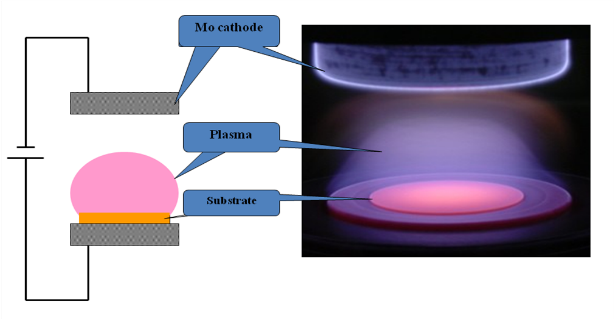
Schema of PE CVD set-up with plasma ball ignited in a methane-hydrogen gas mixture to provide activated carbonaceous species.
Photograph of the PE CVD system at Department of Physics and Mathematics UEF.
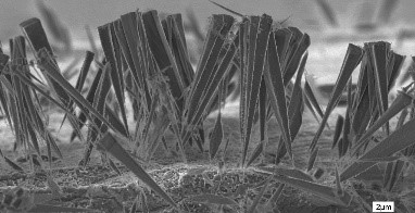
SEM image of the single crystal diamond micro-tips obtained from polycrystalline CVD diamond film by using selective oxidation procedure.
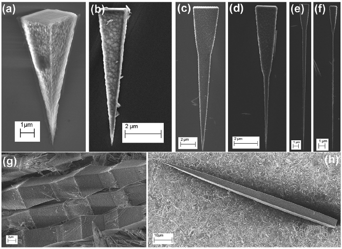
Examples of individual diamond needles with different shapes.
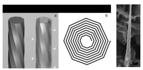
SEM image and scheme of the carbon nano-scrolls having polygonal cross-section.
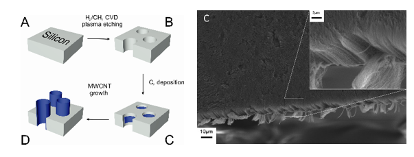
Scheme of growth and SEM image of the carbon nanotube forest on Si porous substrate.
Functional surfaces
Keywords: femtosecond laser ablation; functional surfaces; functional materials
One can have remarkable control of the surface properties by patterning it to contain micro- and nanometer sized structures. In a femtosecond laser ablation those structures are produced with an very short laser pulses that enables precise controlled way to modify the surface topology.
With small structures one can control various functionalities including reflection of light, hydrophobicity, oleophobicity, and even the growth of biological material on the surface. Each functionality requires its own surface structure and proper chemical properties of the surface material. The femtosecond laser provides enough energy in each light pulse so that practically any material from stainless steel to biological tissues can be ablated.
Our team has developed the efficiency of the ablation process by introducing various ways to control the laser beam. These include, e.g., interferometric pattern in ablation and array of beams constructed with diffractive gratings. Also, we have worked successfully in the replication of the structures onto polymer surfaces.
Contact person:
More information about the research
Presentations in Sway
Femtosecond laser ablation
Super hydrophobic surfaces with a femtosecond laser
Making glass hydrophobic
A spherical image of the femtosecond laser laboratory
femtosecond laser laboratory, a spherical image
Externally funded projects:
- FinFem: Nano structures and applications with fs laser technology, 2008-2010. Funded by Tekes, www.tekes.fi
- Multibeam: Multiple laser beam processing in mass production, 2011-2013. Funded by Tekes, www.tekes.fi
- Laser-ablation assisted spectroscopy the diagnostics of plants, 2014. Funded by Tekes/ERF, www.tekes.fi
References:
- Martti Silvennoinen, “Precise material processing with spatial light modulator – controlled femtosecond laser beam”, Publications of the University of Eastern Finland. Dissertations in Forestry and Natural Sciences 148 (2014).
- Jarno Kaakkunen, “Fabrication of functional surfaces using ultrashort laser pulse ablation”, Publications of the University of Eastern Finland. Dissertations in Forestry and Natural Sciences 45 (2011).
- M. Silvennoinen, J. J. J. Kaakkunen, K. Päiväsaari, and P. Vahimaa, “Parallel femtosecond laser ablation with individual controlled intensity”, Opt. Express 22, 2603 (2014).
- K. L. Wlodarczyk, J. J. J. Kaakkunen, P. Vahimaa, and D. P. Hand, “Efficient speckle-free laser marking using a spatial light modulator”, Appl. Phys. A 116, 111 (2013).
- M. Silvennoinen, J. J. J. Kaakkunen, K. Päiväsaari, and P. Vahimaa, “Water spray assisted ultrashort laser pulse ablation”, Appl. Surf. Sci. 265, 865 (2013).
- M. Silvennoinen, J. J. J. Kaakkunen, K. Päiväsaari, and P. Vahimaa, “Parallel microstructuring using femtosecond laser and spatial light modulator”, Phys. Procedia 41, 1875 (2013).
- T. Nuutinen, M. Silvennoinen, K. Päiväsaari, and P. Vahimaa, “Control of cultured human cells with femtosecond laser ablated patterns on steel and plastic surfaces”, Biomed. Microdevices 15, 279 (2013).
- J. J. J. Kaakkunen, M. Silvennoinen, K. Päiväsaari, and P. Vahimaa, “Water-assisted femtosecond laser pulse ablation of high aspect ratio holes”, Phys. Procedia 12, 89 (2011).
- J. J. J. Kaakkunen, K. Päiväsaari, and P. Vahimaa, “Fabrication of large-area hole arrays using high-efficiency two-grating interference system and femtosecond laser ablation”, Appl. Phys. A 103, 267 (2011).
- M. Silvennoinen, J.J.J. Kaakkunen, K. Päiväsaari, P. Vahimaa, and T. Jääskeläinen, “Controlling the hydrophopic properties of material using femtosecond ablations”, J. Laser Micro Nanoeng. 5, 97 (2010).
When laser light is packed to 100 femtosecond of duration the optical power equals power of 30 modern nuclear power plants. When focused down to a micrometer scale focal point the irradiance in the focus becomes trillions times higher than in the core of the Sun where temperature reach 20 million Centigrades.
Pulses of this kind can deform any materials by technology called laser ablation. Though the energy densities of the pulses are enormous the total energy is so low that the pulses do not remarkably heat the sample. With focused pulses a micrometer scale holes can be produced and the material fallen away may form a new types of nanostructures. A surface of this kind may be, e.g., water and dirt repellent and antireflective.
In our femtosecond laboratory many kind of surface materials with various chmical and physical properties can be fabricated. Femtosecond pulses can be also used in production of nanoparticles and in studies of material properties. Also, latest theories on nonstationary optical coherence can be evaluated with ultrashort laser pulses in practice.
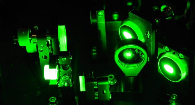
Most important femtosecond laser laboratory tools:
- Quantronix Integra-C 3,5mJ femtosecond laser
- CDP TISSA 50 femtosecond laser
- Grenouille FROG beam analyzer
- CDP ExciPro pump-probe spektrometer
Further information: Pertti Pääkkönen
New materials and surfaces
Keywords: catalysis; chemistry; clay; computational chemistry; coupling chemistry; DFT calculations; friction surfaces; inorganic chemistry; luminescent materials; MAO; material chemistry; metal injection molding (MIM); metallocene; molecular dynamics; molecular modeling; non-covalent interactions; nuclear waste disposal; OLED; organometallic chemistry; photocatalysis; photonics; plastics; polyolefin; quantum chemistry; self-assembly; surfaces; sustainable development; X-ray structural analysis; Ziegler-Natta
The group belongs to the Department of Chemistry and the Center for Photonics Sciences. It is also a member of the Academy of Finland’s Flagship on Photonics Research and Innovation (PREIN).
The group is currently focused on the design, preparation and theoretical analysis of a range of inorganic and organometallic photofunctional molecular materials. The research laboratory is well-equipped for structural and spectroscopic characterization of new compounds with crystallographic and NMR techniques.
In research, the group actively collaborates with international partners from St.-Petersburg State University, National Taiwan University, Technical University of Dortmund, University of Münster, University of Cologne. Our projects are funded by the University of Eastern Finland and the Academy of Finland.
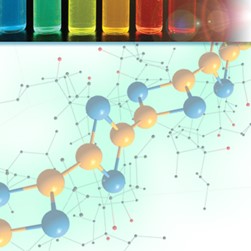
Laboratory
Chemistry laboratories are located at the Futura building (UEF, Joensuu campus). The infrastructure includes, for example, the following devices:
- JNM-EC500 JEOL 500MHz NMR spectrometer: characterization of chemical structure of liquid and solid materials
- Bruker Vertex 70 FTIR spectrometer: characterization of chemical structure of materials
- Elementar Vario Micro series gas chromatography elemental microanalysator: quantitative analysis of nitrogen, sulphur, hydrogen and carbon
- Bruker AXS Kappa Apex Duo, Bruker AXS Smart Apex II, Nonius Kappa Apex single crystal X-ray diffractometers: determination of molecular structures of crystalline materials
- Bruker ACS D8 Advance X-ray diffractometer: characterization of powder crystalline samples
Group in UEF Connect.
Contact people:
Professor, group leader Igor O. Koshevoy
Senior Researcher Pipsa Hirva
Senior Researcher Sirpa Jääskeläinen
Early Stage Researcher Mariia Beliaeva
Early Stage Researcher Iida Partanen
Early Stage Researcher Diana Temerova
Early Stage Researcher Viktoriia Khistiaeva
Selected publications:
- Sivchik, V.; Kochetov, A.; Eskelinen, T.; Kisel, K. S.; Solomatina, A. I.; Grachova, E. V.; Tunik, S. P.; Hirva, P.; Koshevoy, I. O. Modulation of Metallophilic and π–π Interactions in Platinum Cyclometalated Luminophores with Halogen Bonding. Chem. Eur. J. 2021, 27, 1787-1794.
- Lin, T.-C.; Liu, Z.-Y.; Liu, S.-H.; Koshevoy, I. O.; Chou, P.-T. Counterion Migration Driven by Light-Induced Intramolecular Charge Transfer. JACS Au 2021, 1, 282-293.
- Belyaev, A.; Slavova, S. O.; Solovyev, I. V.; Sizov, V.; Jänis, J.; Grachova, E. V.; Koshevoy, I. O. Solvatochromic dual luminescence of Eu-Au dyads decorated with chromophore phosphines. Inorg. Chem. Front. 2020, 7, 140-149.
- Belyaev, A.; Cheng, Y.-H.; Liu, Z.-Y.; Karttunen, A. J.; Chou, P.-T.; Igor O. Koshevoy A Facile Molecular Machine: Optically Triggered Counterion Migration via Charge Transfer of Linear D-π-A Phosphonium Fluorophores. Angew. Chem. Int. Ed. 2019, 58, 13456–13465.
- Belyaev, A.; Chen, Y.-T.; Liu, Z.-Y.; Hindenberg, P.; Wu, C.-H.; Chou, P.-T.; Romero-Nieto, C.; Koshevoy, I. O. Intramolecular Phosphacyclization: Polyaromatic Phosphonium P-Heterocycles with Wide Tuning Optical Properties (420-780 nm emission). Chem. Eur. J. 2019, 25, 6332–6341.
- Shakirova, J. R.; Grachova, E. V.; Gurzhiy, V. V.; Thangaraj, S. K.; Jänis, J.; Melnikov, A. S.; Karttunen, A. J.; Tunik, S. P.; Koshevoy, I. O. Heterometallic cluster-capped tetrahedral assemblies with postsynthetic modification of the metal cores. Angew. Chem. Int. Ed. 2018, 57, 14154-14158.
- Belyaev, A.; Eskelinen, T.; Dau, T. M.; Ershova, Y. Y.; Tunik, S. P.; Melnikov, A. S.; Hirva, P.; Koshevoy, I. O. Cyanide-assembled d10 coordination polymers and cycles: excited state metallophilic modulation of solid-state luminescence. Chem. Eur. J. 2018, 24, 1404–1415.
- Belyaev, A.; Chen, Y.-T.; Su, S.-H.; Tseng, Y.-J.; Karttunen, A. J.; Tunik, S. P.; Chou, P.-T.; Koshevoy, I. O. Copper-mediated phospha-annulation to attain water-soluble polycyclic luminophores. Chem. Commun. 2017, 53, 10954-10957.
- Chakkaradhari, G.; Chen, Y.-T.; Karttunen, A. J.; Dau, M. T.; Jänis, J.; Tunik, S. P.; Chou, P.-T.; Ho, M.-L.; Koshevoy, I. O. Luminescent Triphosphine-Cyanide d10 Metal Complexes. Inorg. Chem. 2016, 55, 2174–2184.
- Sivchik, V. V.; Solomatina, A. I.; Chen, Y.-T.; Karttunen, A. J.; Tunik, S. P.; Chou, P.-T.; Koshevoy, I. O. Halogen Bonding to Amplify Luminescence: A Case Study Using a Platinum Cyclometalated Complex. Angew. Chem. Int. Ed. 2015, 54, 14057–14060.
Photocatalysis Research Group
The photocatalysis research group is a part of Functional Surfaces research topic at the Department of Chemistry in the University of Eastern Finland. The group is also a member of the UEF Photonics Research Community and a member of the Academy of Finland Flagship on Photonics Research and Innovation (PREIN).
Photocatalysis utilizes light to activate chemical reactions. The most studied photocatalytic material is titanium dioxide (TiO2), which is a widely used white, inert, and non-toxic pigment and semiconductor. The bandgap of TiO2 is 3.2 eV corresponding to the UVA-range that is only approximately 3-5% of the solar spectrum. Therefore, recent research has focused on functionalization of TiO2 structures, for example, with metal nanoparticles that can couple visible light wavelengths for the photocatalytic excitation via plasmonic coupling. This can significantly improve the efficiency of such metal-semiconductor composites.
Our research group concentrates on fabrication and characterization of TiO2 inverse opal structures functionalized with different metallic nanostructures that allow efficient solar-driven chemical reactions and improved hydrogen evolution.
Laboratory
The photocatalysis laboratory is located at the Futura Building in the UEF Joensuu campus. The laboratory is equipped with novel gas-phase photocatalytic activity characterization tools and possibilities for various synthesis routes for multicompound and multilayer inverse opal semiconductor structures. The infrastructure includes measuring, imaging and manufacturing devices, for example:
- Renishaw inVia confocal Raman microscope: chemical structure of materials as a function of sample depth, surface-enhanced Raman spectroscopy
- Hitachi S-4800 FE-SEM scanning electron microscope with Thermo Electron Noran System Six 200 EDS detector: examination of surface structures of materials in micro and nanometer scale and measurement of elemental composition
- Perkin Elmer Lambda 900 UV/VIS/NIR spectrometer: characterization of chemical structure of materials and measurement of colour, transmission and reflection properties
- JNM-EC500 JEOL 500MHz NMR spectrometer: characterization of chemical structure of liquid and solid materials
- Bruker Vertex 70 FTIR spectrometer: characterization of chemical structure of materials
- KSV Cam 200 Contact angle meter: wettability of materials, contact angle and surface tension
- KVS NIMA Dipcoater and Laurell technologies Co WS-400A-6NPP/LITE/10K spin coater: coating of materials with solutions
- Cressington 208HR high resolution sputter coater: coating of materials with thin metal layer for SEM measurements
- Haake MiniJet Micro compounder and Haake MiniLab micro Mini injection molding device: injection molding in laboratory scale and preparation of test specimen
- Oxford Instruments Plasmalab 80plus ICP-DRIE plasma system: tailoring of surface structure and chemistry of materials
- An in-house-built gas-phase photoreactor for photocatalytic activity characterization (measured by degradation of C2H2 into CO2 that is directly detected by an optical detector (Vaisala GMP343 diffusion mode) inside the photoreactor)
- XRD by Bruker-AXS D8 Advance device
Group members
An automatically updated list of personnel can be found from the group UEF Connect website.
Publications
Our recent publications can be found from the group UEF Connect website.
Further information: Jarkko J. Saarinen
Laboratory
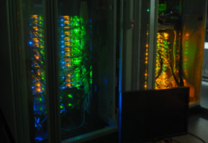
The infrastructure includes computer clusters located at the Futura building (UEF, Joensuu campus):
- Dell EMC PowerEdge – 1240 cores
- HP ProLiant – 768 cores
- Dell PowerEdge – 768 cores
The computer clusters are combined into a grid of computer clusters situated at different locations around Finland (The Finnish Grid and Cloud Infrastructure). The joint resources are part of the cPouta cloud.
For more information, see group UEF Connect page.
 |
 |
We work in two complementary directions:
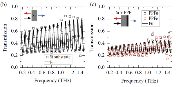
- We study electromagnetic response of carbon-based materials using the time-domain spectroscopy tool and home-made Fourier transform spectrometers. The latter are also used to study the THz emission of optically pumped structures and materials.
- We study the photoresponse (photoconductivity, photovoltage) of graphene and CNT based nano and microstructures.
One of the main motivations is study of low-energy collective and single particle excitations in materials and nanostructures.
The applied research is centered on developing novel optical and optoelectronic components for terahertz range. Those include but are not limited to on-chip spectrometers, compact THz radiation sources, advanced biosensors.
Reference
https://doi.org/10.1016/j.carbon.2021.09.067
https://doi.org/10.1016/j.carbon.2021.10.054
https://doi.org/10.1088/1361-6528/ac3861
https://doi.org/10.1103/PhysRevApplied.17.044041
https://doi.org/10.3952/physics.2023.63.3.6
Contact persons:
Dr. Georgy Fedorov
Prof. Polina Kuzhir
Prof. Yuri Svirko
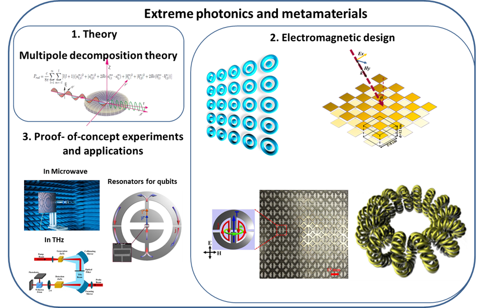
High Q-factor resonances driving numerous phenomena in electromagnetics, nanophotonics and quantum communication are in focus of our study. High Q cavities based on meta-particles and metamaterials enable to excite resonances associated with the nonrading states such as anapoles and bound states in the continuum. These resonances are enhanced in the close proximity of the subwavelength object, while it is nullified in the far-field zone. Our study aims at development of a novel methodology based on multipole decomposition approach for designing THz and microwave metamaterials with extremely high Q-factor resonances. We target to transparent metasurfaces, invisible particles, highly sensitive detectors, bolometers, and resonators for qubits.
References:
- A. Ospanova, M. Cojocari, P, Lamberti, A. Plyushch, L. Matekovits, Y. Svirko, P. Kuzhir, A. Basharin, “Broadband transparency of Babinet complementary metamaterials”, Applied physics letters, 122 , 231702 (2023).
- A. Ospanova, M. Cojocari, and A. Basharin, “Modified multipoles in photonics”, Phys. Rev. B 107, 035156 (2023).
Contact persons:
Dr. Alexey Basharin
Prof. Polina Kuzhir
Quantum materials
Keywords: nanodiamonds; color centers; N-V centers; quantum sensing; quantum imaging; SiV centers; GeV centers
Diamonds with NV and other color centers are key for solid-state room-temperature quantum technologies including sensing, communications and calculations. We’re refining chemical vapor deposition (CVD) diamond synthesis to enhance quality and control centers distribution for quantum applications. Single crystal diamond needles (SCDNs) are particularly promising for precise quantum sensors, combining nanoscale sensitivity with ease of handling, and we’re advancing their production and integration of various color centers, and investigating their prospects in quantum applications.
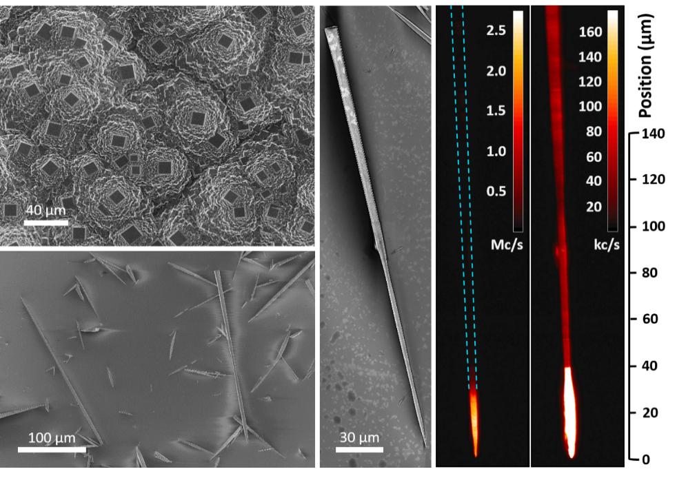
Scanning electron microscopy images of carbon film contained SCDNs in its structure (a top), extracted SCDNs on a silicon plate (a bottom), individual SCDN (b) and confocal PL maps of individual SCDN (c, d) obtained with 740(10) bandpass filter. The dark rectangles in the (a top) are bases of the SCDNs. The PL maps (c and d) are for the same data and differ only in the maximum displayed intensity level. The Mc/s and kc/s in the scales indicate megacounts and kilocounts of photons per second respectively. The blue dashed lines in (c) present the outline of the SCDN.
Contact persons:
Prof. Polina Kuzhir
Dr. Sergei Malykhin
Prof. Alexander Obraztsov
Selected publications:
- R. Ismagilov, S. Malykhin, A. Puzyr, A. Loginov, V. Kleshch, and A. Obraztsov, “Single-crystal diamond needle fabrication using hot-filament chemical vapor deposition”, Materials 14, 2320 (2021).
- L. Arnoldi, M. Borz, I. Blum, V. Kleshch, A. Obraztsov, and A. Vella, “Effect of laser illumination on the electrical conductivity of single-crystal diamond needles”, J. Appl. Phys. 126, 045710 (2019).
- S. Malykhin, Y. Mindarava, R. Ismagilov, A. Orekhov, F. Jelezko, and A. Obraztsov, “Formation of GeV, SiV, and NV color centers in single crystal diamond needles grown by chemical vapor deposition”, Phys. Status Solidi B Basic Res. 256, 1800721 (2019).
- L. Venturi, L. Rigutti, J. Houard, I. Blum, S. Malykhin, A. Obraztsov, and A. Vella, “Strain sensitivity and symmetry of 2.65 eV color center in diamond nanoscale needles”, Appl. Phys. Lett. 114, 143104 (2019).
- S. Malykhin, Y. Mindarava, R. Ismagilov, F. Jelezko, A. Obraztsov, “Control of NV, SiV and GeV centers formation in single crystal diamond needles”, Diamond & Related Materials 125, 109007 (2022).
- S. Malykhin, et. al. “Photoluminescent properties of single crystal diamond microneedles”, Opt. Mat. 75, 49 (2018).
- M. Quarshie, S. Malykhin, A. Obraztsov, P. Kuzhir, “Nano- and micro-crystalline diamond film structuring with electron beam lithography mask”, Nanotechnology 35 155301 (2024).
- M. Quarshie, S. Malykhin, and P. Kuzhir, “Core-shell diamond-graphene needles with silicon-vacancy color centers”, Opt. Mat. Express 14, 965 (2024).
Keywords: Nanodiamonds, color centers, N-V centers, quantum sensing, quantum imaging, SiV centers, GeV centers