Optical components and their precision manufacturing
3D printed photonics and free-form optics
Keywords: 3D printing; additive;manufacturing;freeform optics; graded-index optics (GRIN)
3D printing (also known as additive manufacturing) is considered a third industrial revolution. Although multiple examples in aerospace, architecture, automotive, biotech (human tissue replacement), dental and medical industries, education, eyewear, fashion, footwear, industrial design, jewellery, military, food etc., the area that has been missing is optics. Dutch start-up Luxexcel is the exception to the statement. They have invented the Printoptical® technology for 3D printing optical elements. Their technology is based on an inkjet printing process.

In collaboration with Luxexcel, our group will further develop the Printoptical® technology towards smaller features and more accurate surface control, larger selection of materials, novel optics and unique combination with other state-of-the-art micro-optics and nano photonics manufacturing methods as well as mechanics, electronics and biocompatible materials.
Until recently, because of over hundred years old manufacturing methods, optical elements have been either rotationally or linearly symmetric. Thanks to the progress of Computer Numerical Control (CNC) machines, freeform surfaces that depart from rotational symmetry for use at the wavelengths as short as one micron is possible. Freeform optics introduces innovative 3-dimensional solutions: one element contains more complicated and numerous optical functions with better performance than ever before. Thanks to freeform optics, optical system development is entering into the era of revolution.
Because of the nature of 3D printing (adding structured layers on top of each other), the method is ideal for freeform optics. Actually, 3D printing complicated freeform optics is as easy or difficult as printing perfect spherical lenses – “complexity is free” in 3D printing.
Novel strategies and algorithms based on our expertise in diffractive optics and results of forthcoming 3D printing experiments will be developed for free-form optics design. We aim at synthesizing design concepts in diffractive and free-from optics, and to develop hybrid optical elements and systems that employ both technologies.
Contact persons:
Prof. Jyrki Saarinen
Prof. Markku Kuittinen
Dr. Petri Karvinen
Dr. Pertti Pääkkönen
MSc Markku Pekkarinen
Externally funded projects:
- Photonics 4.0, the Federation of Finnish Technology Industries and Jane and Aatos Erkko Foundation, 2019-2021
- Reference algorithms and metrology on aspherical and freeform optical elements (FreeFORM), European Commission, 2016-2019
- Three-dimensionally printed optics, Academy of Finland, 2015-2019
- ACE 3D – Accurate, cost-effective and easy 3D printing for MedTech component production, Business Finland, 2018
- OPTI-PRO – Nanohybrid lens with integrated nanostructures for professional industrial applications, Tekes, 2017 – 2018
- Freeform optics from prototyping to volume production (FOPRO2), Tekes, 2015-2017
- 3D Printed Photonics – Phase I (3DPPI), Tekes, 2013-2015
Academic partners (present and former):
Industrial partners:
Nanobakers
See also
Characterization
In addition to micro and nano scale fabrication a larger scale fabrication methods are needed. For this purpose the mechanical laboratory includes lapping, grinding and polishing machinery.
In the electronics laboratory we are able to design, fabricate and repair electronic tools and devices. A CNC milling machine and soldering stations enable design and fabrication of PCB’s. For harder machinery there is a well equipped mechanic workshop with turning and cutter machines as well as welding machines. Together these workshops form an unit which is essential when maintaining the research infrastructure.
Further information: Pertti Pääkkönen
Albeit the function of an optical micro and nanostructure can be numerically modeled, its performance must be verified optically. Our well equipped optical laboratories serves for this purpose.
In the optical laboratories there are various laser and LED light sources for different applications. Light properties can be modified by lenses, beam splitters and polarizing components. Light properties can be analysed using different interferometric setups, spectrometers, light detectors and cameras.
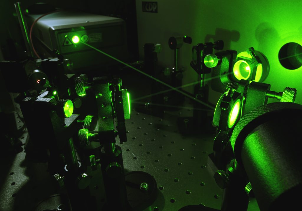
Most important optical laboratory tools include:
- Woollam VASE ellipsometer
- Perkin Elmer spectrophotometers
- Solartron 1260A impedance analyzer
- KSV Instruments contact angle meter
- Toptica spectrum analyzer
Further information: Pertti Pääkkönen
Because optical structures to be studied are in micro or nanometer scale, conventional microscopes or mechanic measuring is not adequate methods for studies of this scale. For measuring and analyzing of these structures our characterization laboratory is equipped also with electron and atomic force microscopes.
Characterization is crucial also within lithographic fabrication methods. Often it is necessary to verify success of a fabrication step prior to proceeding to the next step. Because of this our characterization laboratory is integrated with lithographic laboratory in our cleanroom laboratory.
Characterization laboratory equipment is suitable for other types of surface inspection. Our facilities can be also used to study almost any surfaces for chemistry, material science, medical, bio science or nanotechnology needs.
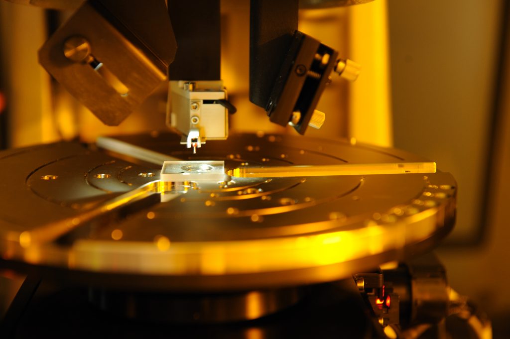
Most important characterization tools:
- LEO 1550 electron microscope
- Dektak 150+ surface profiler
- Wyko NT9300 optical profiler
Further information: Pertti Pääkkönen
Micro- and nanophotonics
Keywords: micro- and nanophotonics; nanofabrication; metrology; cleanroom; lithography; graphene; carbon nanotube; Terahertz; microwave; electromagnetic; detector; bolometer; metamaterial; metasurface;
Department has modern clean room facilities for the fabrication of micro- and nanostructures including equipment for resisting, patterning, etching, and thin film coating. The patterning is performed by using an electron beam pattern generator, Ebeam EBPG5000+ES HR (Vistec) or by interferometric exposure.
The photonic structures can be metallic or dielectric ones, depending on application. The laboratory is equipped also with electroplating and nanoimprinting systems allowing flexible copying of structures on various materials.
Contact person: Markku Kuittinen
Fabrication of optical micro and nanostructures requires an environment where particles, temperature and humidity are carefully controlled with effective air conditioning.
Cleanrooms at Joensuu campus are built in three phases. First 25 m2 were built in year 1995 and next 35 m2 in year 1997. Third 120 m2 cleanrooms joining the first two ones into single cleanroom unit were built in year 2006. Together with cleanroom service areas the total area of cleanroom laboratories is about 200 m2.
The cleanroom is an environment for many technologies used in optical structures fabrication:
- Electron Beam Lithography
- Nanoimprint Lithography
- Reactive Ion Etching
- Thin Film fabrication
- Nickel Electroplating
- Scanning Electron Microscopy
Newest cleanrooms makes use of modern cleanroom technology.
Click to visit virtually in our cleanroom facilities
Further information: Pertti Pääkkönen
When light propagation is to be controlled accurately the surfaces used need to be prepared with nanometer scale accuracy. In the Department of Physics these surfaces are fabricated using electron beam lithography and holographic laser lithography.
These micro and nano structures are designed using latest numerical computation methods. Structures which often looks random, are realized in quartz, silicon, lithium niobate etc. substrates using various physical and chemical lithographic methods. In addition to lithographic methods we have various supporting technologies such as reactive ion etching (RIE), thin film evaporation, nickel electroplating, nanoimprint lithography (NIL), etc. Since 1995 our research is focused on development of these methods for micro and nano optics.
The structures to be fabricated are often smaller than dust particles in common room air. Also, the fabrication methods are often sensitive to temperature and air humidity changes. Therefore lithography laboratory operates in the Department clean room where the air quality is carefully controlled.
Most important lithographic technologies:
- Electron beam patterning tool EBPG5000+ES
- Obducat Eitre 3 nanoimprint tool
- Plasmalab 100 ja 80 reactive ion etching tools
- Kurt J. Lesker LAB 18 Physical Vapour Deposition
- Beneq TFS-200 Atomic Layer Deposition
- PTMTEC R2R100UV roll-to-roll printer
- Disco DAD3240 wafer dicing saw
Further information: Pertti Pääkkönen
We concentrate on the theory, modeling and fabrication of THz and microwave devices based on graphene and graphene related 2D materials. The tunability of the electromagnetic response vs biasing, laser irradiation and mechanical deformations has been achieved. The main physical principles making a basis for using carbonaceous thin films as the major working elements of passive microwave-to-THz devices, such as shields, filters, polarizers, collimators, are proposed theoretically and proved experimentally. The proof-of-concept for a tunable radiation-tolerant graphene based THz detector (bolometer and field-effect-transistor type) have been published as public deliverable of ATTRACT EU funded project. Along with the main focus towards astrophysics, proposed feasible and easy to use techniques / protocols might invest into societal challenges with effective detecting of low concentrations of different chemicals/molecules/pollutants, etc.
Group also focus on electromagnetic response of 3D printed architectures coupled with graphene and other carbon films, or metasurface made of carbon nanotubes.
The group have well-established and long-lasting research cooperation with international partners from Institute for Nuclear problems of Belarusian State University (Minsk, Belarus); Vilnius University &Center for Physical Sciences and Technology (Vilnius, Lithuania); University of Namur (Namur, Belgium); Institute of Electronic Structure and Laser (Heraklion, Greece); Universita Degli Studi di Salerno (Salerno,Italy); Moscow Institute of Physics and Technology (Moscow, Russia); University of Exeter and University of Southampton (UK); Universite De Lorraine (Epinal, France); Udmurt Federal Research Center of the UB RAS (Izhevsk, Russia).
This activity is funded by the Academy of Finland and EC Horizon 2020 projects MSCA-RISE-2020 project nr. 101007896 CHARTIST, H2020-MSCA-IF-2018, project nr. 836816 TURANDOT, H2020-MSCA-RISE-2018 project nr. 823728 DiSeTCom, EU.1.4.2.1. ATTRACT project nr. 777222 subproject ROTOR.
Contact persons:
Prof. Yuri Svirko
Prof. Polina Kuzhir
Selected publications:
- A. C. Tasolamprou, A. D. Koulouklidis, C. D., C. P. Mavidis, G. Kenanakis, G. Deligeorgis, Z. Viskadourakis, P. Kuzhir, S. Tzortzakis, M. Kafesaki, E. N. Economou, and C. M. Soukoulis, “Experimental demonstration of ultrafast THz modulation in a graphene-based thin film absorber through negative photoinduced conductivity”, ACS Photonics, 6, 720 (2019).
- A. Paddubskaya, M. Demidenko, K. Batrakov, G. Valušis, T. Kaplas, Y. Svirko, and P. Kuzhir, “Tunable perfect THz absorber based on a stretchable ultrathin carbon-polymer bilayer”, Materials 12, 143 (2019).
- P. Kuzhir, A. Paddubskaya, J. Macutkevic, M. Letellier, A. Celzard, V. Fierro, T. Kaplas, and Y. P. Svirko, “Electromagnetics of carbon: Nano versus micro”, Carbon-Based Nanoelectromagnetics 1, 191 (2019).
- G. Gorokhov, D. Bychanok, P. Kuzhir, D. Gorodetskiy, A. Kurenya, O. V. Sedelnikova, L. Bulusheva, and A. Okotrub, “Creation of metasurface from vertically aligned carbon nanotubes as versatile platform for ultra-light THz components”, Nanotechnology 31, 25570 (2020).
- D. Bychanok, G. Gorokhov, A. Plyushch, A. Ronca, M. Lavorgna, H. Xia, P. Lamberti, and P. Kuzhir, “Terahertz optics of materials with spatially harmonically distributed refractive index”, Materials 13, 5208 (2020).
- A. Paddubskaya, K. Batrakov, A. Khrushchinsky, S. Kuten, A. Plyushch, A. Stepanov, G. Remnev, V. Shvetsov, M. Baah, Y. Svirko, and P. Kuzhir, “Outstanding radiation tolerance of supported graphene: towards 2D sensors for the space millimeter radioastronomy”,
Nanomaterials 11, 170 (2021). - Kuzhir, A. Paddubskay, D. Bychanok, A. Liubimaud, A. Ortona, V. Fierro, and A. Celzard, “3D-printed, carbon-based, lossy photonic crystals: Is high electrical conductivity the must?”, Carbon 171, 484 (2020).
Keywords: graphene, carbon nanotube, Terahertz, microwave, electromagnetic, detector, bolometer, metamaterial, metasurface
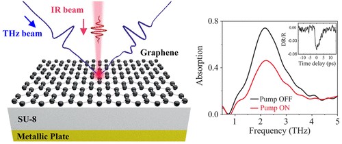
Schematic representation of the graphene absorber structure. It is composed of a graphene monolayer on top of a dielectric (SU-8) film of thickness d = 20 μm placed on a metallic back-reflector. The THz beam illuminates the sample at an angle θ while the sample is optically excited by a near-IR beam at normal incidence.
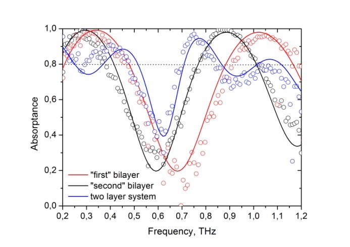
Absorptance spectra of pyrolytic carbon/polymer/gold and pyrolytic carbon/polymer/ pyrolytic carbon/polymer/gold sandwich-like structures.
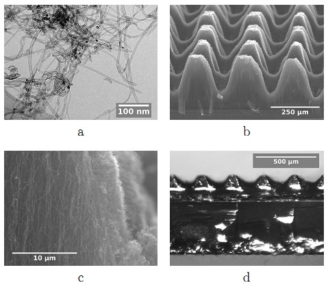
a) TEM image of MWCNTs obtained by CVD technology; (b, c) SEM images of MWCNT-based pyramids periodic array ; (d) Image of the general view of arrays covered with epoxy layer.

