Research / Optical components / Lithography laboratory
When light propagation is to be controlled accurately the surfaces used need to be prepared with nanometer scale accuracy. In the Department of Physics these surfaces are fabricated using electron beam lithography and holographic laser lithography.
These micro and nano structures are designed using latest numerical computation methods. Structures which often looks random, are realized in quartz, silicon, lithium niobate etc. substrates using various physical and chemical lithographic methods. In addition to lithographic methods we have various supporting technologies such as reactive ion etching (RIE), thin film evaporation, nickel electroplating, nanoimprint lithography (NIL), etc. Since 1995 our research is focused on development of these methods for micro and nano optics.
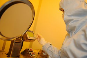
The structures to be fabricated are often smaller than dust particles in common room air. Also, the fabrication methods are often sensitive to temperature and air humidity changes. Therefore lithography laboratory operates in the Department clean room where the air quality is carefully controlled.
 |
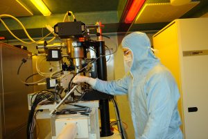 |
Most important lithographic technologies:
- Electron beam patterning tool EBPG5000+ES
- Obducat Eitre 3 nanoimprint tool
- Plasmalab 100 ja 80 reactive ion etching tools
- Kurt J. Lesker LAB 18 Physical Vapour Deposition
- Beneq TFS-200 Atomic Layer Deposition
- PTMTEC R2R100UV roll-to-roll printer
- Disco DAD3240 wafer dicing saw
Further information: Pertti Pääkkönen